Coatings with individual possibilitiesSputtering targets
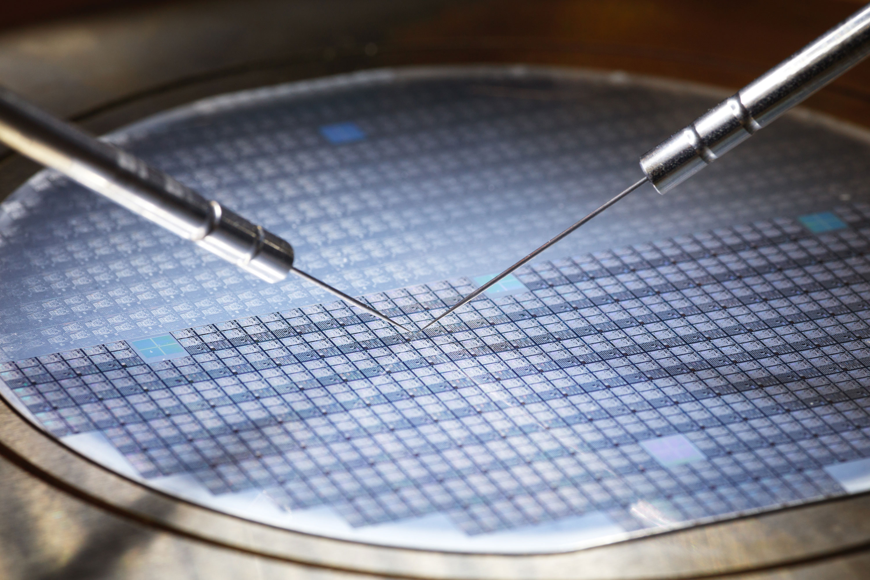
Sputtering targets made of mono- and multicrystalline silicon can be used to apply functional, "configurable" silicon layers to various materials. The more high-grade these coatings are to be, the more important the quality of the sputtering targets: Material purity and manufacturing quality are key success factors. At the same time, a specifically tailored combination of target material, doping and resistivity, as well as back plate / heat sink plays a central role – together with the appropriate bonding process and the shape and size of the entire target.
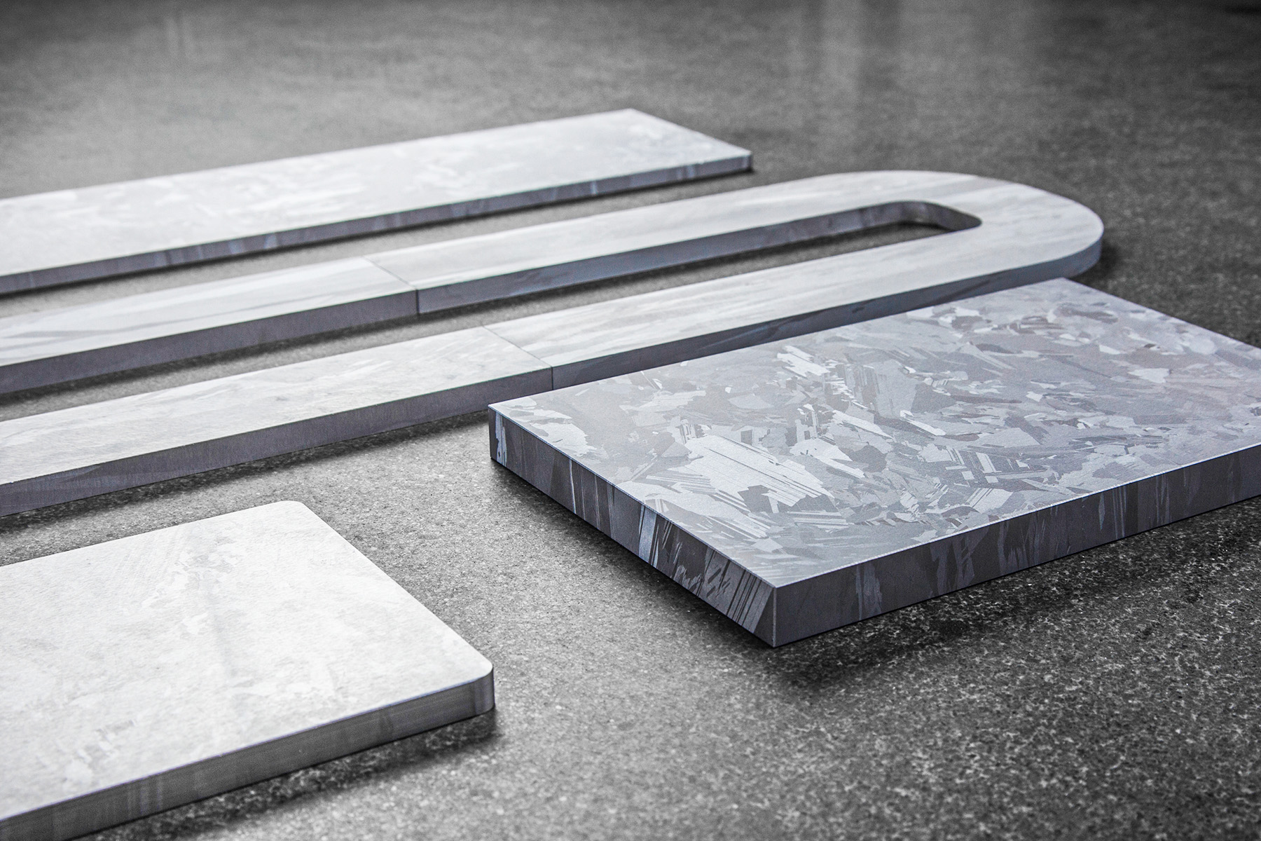
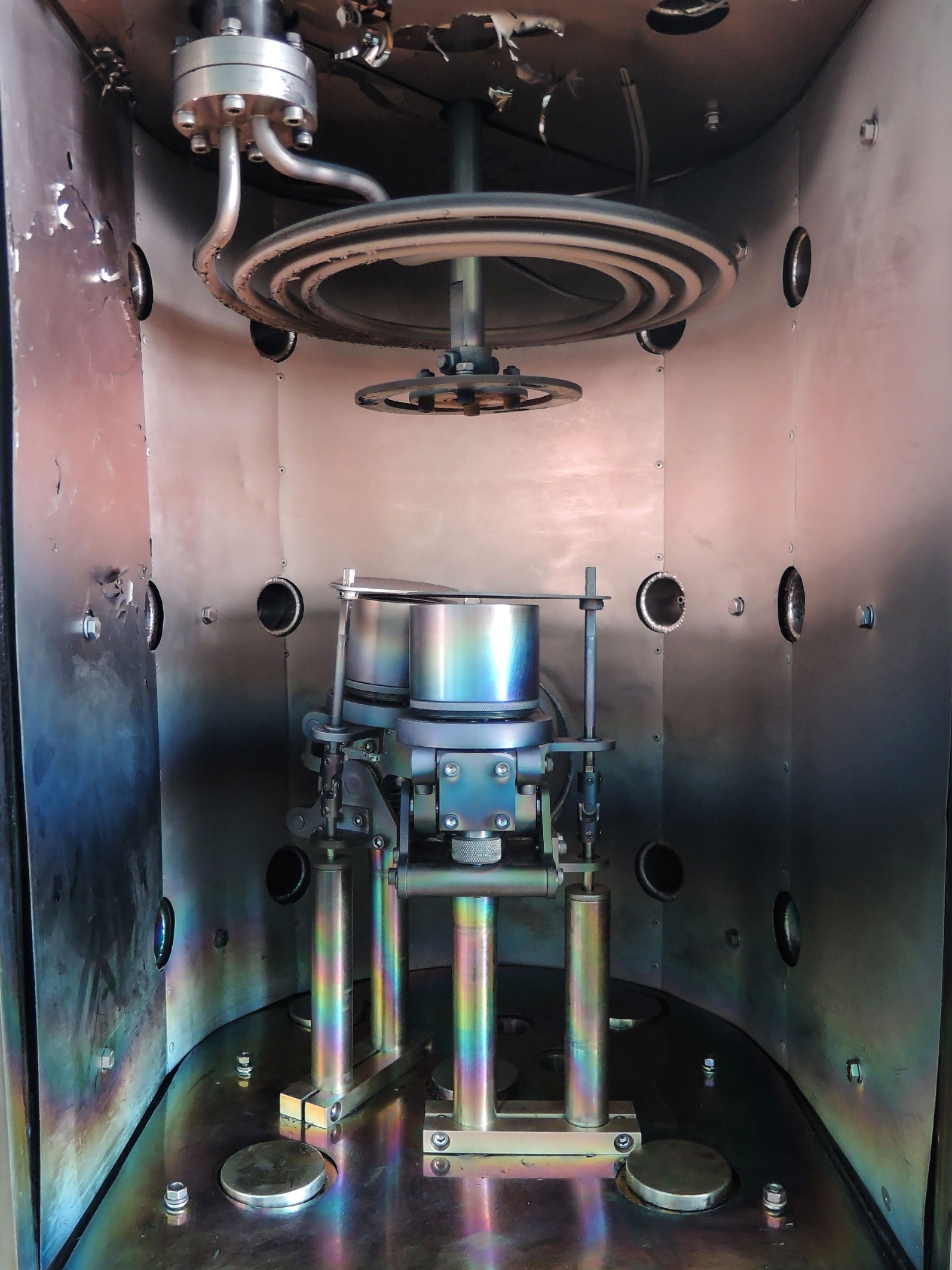
Consistently high quality and abundant flexibility: Drawing on our vast experience and in close contact with our customers, we manufacture high-purity mono- or multicrystalline sputtering targets that are a perfect fit for your project, because an ideal coating needs the right interaction of sputtering targets, cathode and the relevant individual parameters. We manufacture the sputtering targets individually for your specific application. In doing so, we tailor the exact configuration of the target in detail: Geometry, possibly a heat sink and back plate, and an optional appropriate bonding process permit specific target properties. Various individually tailored n-type and p-type doping processes – with boron (p-type) or phosphorus, arsenic and antimony (n-type), for instance – round off the configuration options – the fitting response to the increasingly individual demands being placed on functional coatings. We permanently monitor the quality of every single batch with a trained eye. The result: Silicon targets for absolutely uniform, durable coatings on a wide variety of materials – for specifically improved material properties or tailor-made functional layers. Typical areas of application include photovoltaics, the optical and optoelectronics industry, the semiconductor technology sector and sheet-glass manufacturing, but they are also used in many branches of research and development, such as for testing the characteristics of new material compositions or conducting scientific experiments.
Application cases
Coating of various materials
Enhancement of material properties
Manufacturing of functional layers
Technical data
| Monocrystalline silicon | Dopants | Arsenic, phosphorus, antimony (n-type); boron (p-type) |
| Purity | ≥5N / ≥99.999% | |
| Resistivity | 0.01–1,000 ·cm | |
| Crystal orientation | 111> & 100> | |
| Dimensions, single piece | max. Ø 450 mm, max. ◻ 320×320 mm | |
| Size when segmented | according to customer requirements | |
| Thickness | 1 mm to >14 mm | |
| Multicrystalline silicon | Dopant purity | Phosphorus (n-type), boron (p-type) ≥5N / ≥99.999% |
| Resistivity | 0.01–3 ·cm | |
| Dimensions, single piece | max. Ø 780 mm, max. ◻ 780×780 mm | |
| Size when segmented | according to customer requirements | |
| Thickness | 1 mm to >14 mm |